GaP Wafer, undoped (111) 2"x0.4 mm, 2sp,

GaP Wafer, undoped (111) 2"x0.4 mm, 2sp,

RM0.00 MYR
Sale price  RM0.00 MYR Regular price 
Skip to product information
GaP Wafer, undoped (111) 2"x0.4 mm, 2sp,

GaP Wafer, undoped (111) 2"x0.4 mm, 2sp,

SKU: gap-wafer-undoped-111-2x0-4-mm-2sp

Price: RFQ

Description

GaP single crystal wafer, Size: 2" diameter x 0.4mm, Doping: undoped Conducting type: Orientation: (111) Polished: two sides polished with P terminated side facing down in the box. Surface finish (RMS or Ra) : < 8A Typical Physical Properties Crystal Structure Cubic. Growth Method CZ (LEC) Density Mobility: 150cmE2/Vs Thermal Expansion Dopant undoped Crystal growth axis <111> Conducting Type N Carrier Concentration 2.7 x10 16 /cm 3 Resistivity 1.53 ohm.cm EPD 3.4x10 4 Related Product Other Crystal wafer A-Z Plasma Cleaner Wafer Containers Dicing saw Film Coater

Typical Physical Properties

Crystal Structure

Cubic.           

Growth Method

CZ (LEC)

Density

Mobility:

150cmE2/Vs

Thermal Expansion


Dopant

undoped

Crystal growth axis

<111> 


Conducting Type

N


Carrier Concentration

2.7 x10¹⁶ /cm3

Resistivity

1.53 ohm.cm


EPD

3.4x10⁴

,

Other Crystal wafer A-Z

Plasma Cleaner

 Wafer Containers

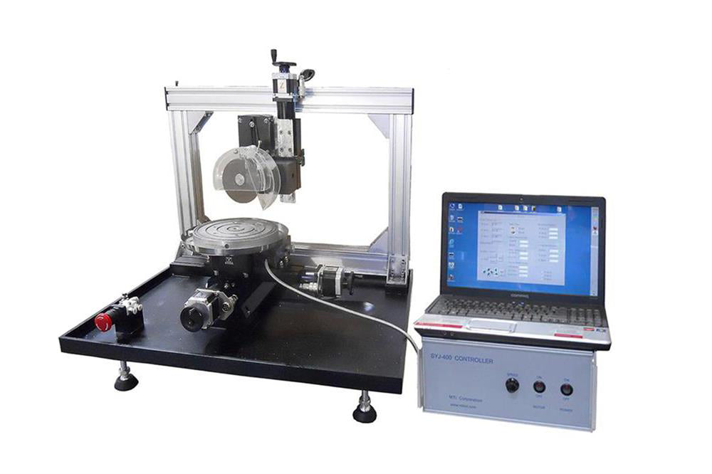
Dicing saw

Film Coater