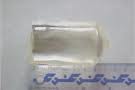
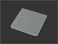
GaN -Single Crystal Substrate (0001), 50.8mm x 0. 25 mm , N+ type, 2SP

GaN -Single Crystal Substrate (0001), 50.8mm x 0. 25 mm , N+ type, 2SP

RM0.00 MYR
Sale price  RM0.00 MYR Regular price 
Skip to product information
GaN -Single Crystal Substrate (0001), 50.8mm x 0. 25 mm , N+ type, 2SP

GaN -Single Crystal Substrate (0001), 50.8mm x 0. 25 mm , N+ type, 2SP

SKU: gan-single-crystal-substrate-0001-50-8mm-x-0-25-mm-n-type-2sp

Price: RFQ

Description

GaN single crystal substrates is made by a hydride vapor phase epitaxy (HVPE)-based method. During the HVPE process, HCl reacts with molten Ga to form GaCl, which in turn reacts with NH3 to form GaN. The large growth rate enables the growth of self-supporting wafer thicknesses in a convenient time period.

Specifications of Substrate 

  • Orientation: c-axis (0001) +/- 1.0 o
  • Nominal Thickness: 250+/- 50 um
  • Dimension: 50.8mm+/-1mm
  • Bow: <5 microns
  • TTV: <10 microns
  • Conduction Type: N+ type
  • Resistivity: < 0.05 Ohm-cm
  • Dislocation Density: < 5x106cm-2
  • Macro Defect Density: < 5 cm-2
  • Transmission: => 70% 
  • Front Surface Finish: (Ga Face) , Epi-ready,RMS <1 nm
  • Back surface finish: N-face Epi-ready,RMS <1 nm                                  
  • Edge Exclusion Area: 1 mm
  • Carrier Concentration: >5E17/c.c
  • Package Single Wafer: Container or membrane box 


Other Sapphire

GaN

 AlN template 

ZnO

A-plane (11-20)

Diamond Scriber

Vacuum Pen

Wafer Containers

Film Coaters